You are currently viewing A Programmable Voltage Calibrator

A Programmable Voltage Calibrator

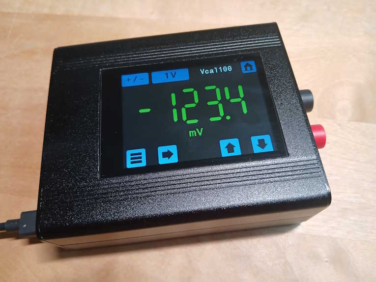
When working on electronic circuits it is sometimes quite useful to be able to apply a precise voltage with only a few mA of current. If the required resolution goes down into the mV region, a lab power supply is usually not good enough for this purpose. This calls for a voltage calibrator which I am going to build as my next project.

Features

  • Resolution 1 mV or better
  • 10V range
  • Unipolar and bipolar operation
  • Exact zero
  • Load correction
  • Gain and Offset
  • Limiting function
  • Remote control via USB without any special drivers
  • Touch screen
  • Compact design

Schematic

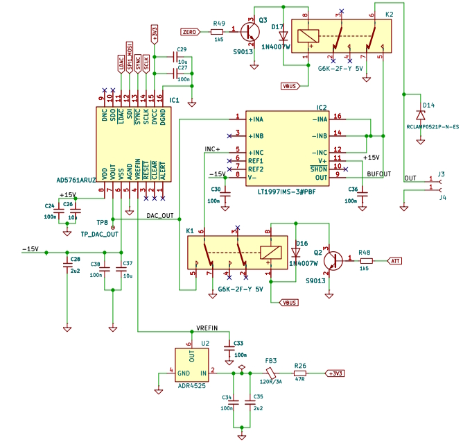
The device is built around the 16-bit DAC AD5761 from Analog devices. It receives settings from the MCU via its SPI interface.

The reference source is a low noise, low drift ADR4525. The output of the DAC is fed into a precision amplifier LT1997-3 which can be configured to have a gain of 1 or 0.1 by switching relay K1. Relay K2 can short the output to guarantee an output voltage of exactly 0 Volt regardless of any offset voltage the circuit may have. A bipolar TVS diode protects the output against electrostatic discharge.

DAC and Output Buffer

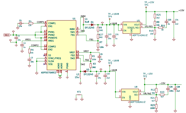
The analog circuitry needs power supply voltages of -15V and +15V. An ADP5070 switching regulator creates voltages ±16.8V from the 5V of the USB interface. These voltages are then filtered by the low noise linear regulators ADP7142 and ADP7182 to get approximately ±15V.

Power Supply

Ranges

The AD5761 includes a configurable output amplifier. With a 2.5V reference and by configuring gain and offset of this amplifier these ranges can be set:

±10V / ±5V / ±3V / −2.5V to +7.5V / 0V to 20V / 0V to 16V / 0V to 10V / 0V to 5V.

Of these we are only using ranges ±10V / ±5V / 0V to 10V and 0V to 5V here. Together with the attenuator switch this gives us ranges 0.5V / 1V / 5V / 10V, unipolar or bipolar.

The AD5761 has an overrange option by which the nominal ranges can be extended by 5%. I am using this option to make sure each range is fully covered and to also leave some headroom for calibration.

Taking the 5% overrange into account we get the following values for the granularity at the output.
RangeGranularity [mV/step]
±10V0.32
±5V0.16
±1V0.032
±0.5V0.016
10V0.16
5V0.08
1V0.016
0.5V0.008

As can be seen, the targeted resolution of 1 mV should be feasible for all ranges. For ranges ±1 V and below we may even go for a resolution of 0.1 mV.

Calibration

Using a digital multimeter with remote control the device can be calibrated using a simple Python skript which is included in the download package.

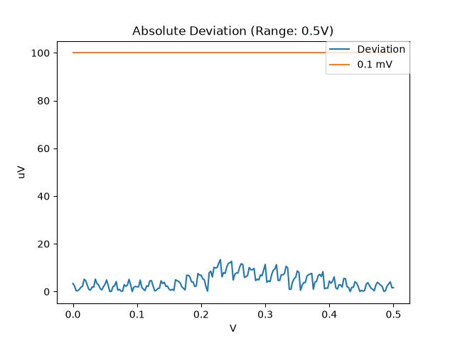
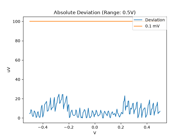
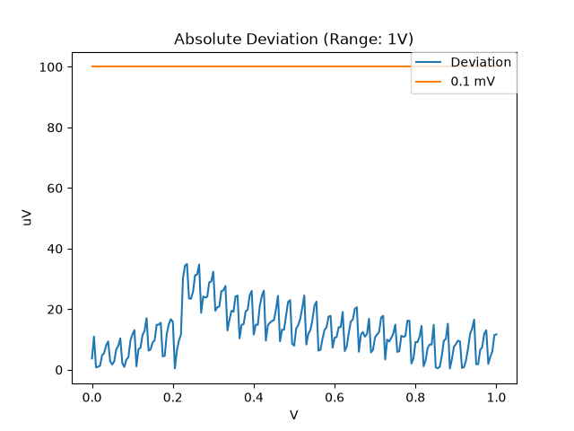
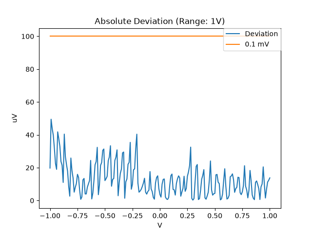
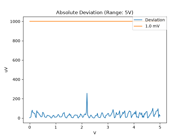
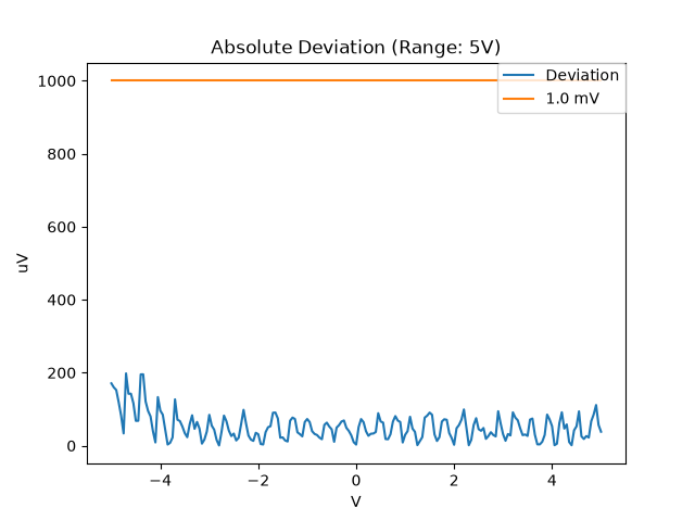
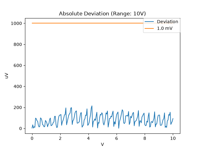
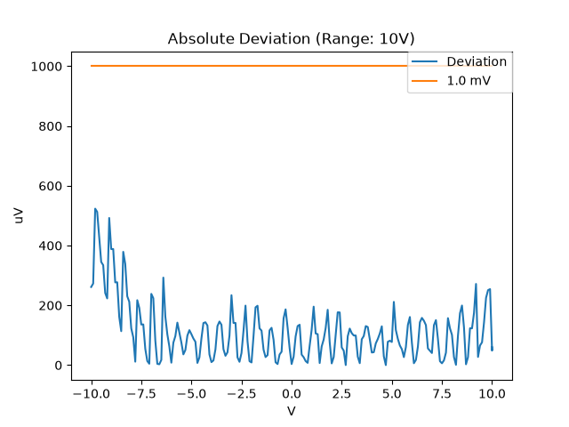
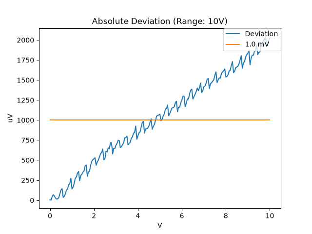
Test Results (RL=open)

These are results of test runs over all ranges with unipolar (left) and bipolar (right) polarities.   

Load Correction

The internal resistance of the device is small but finite. Therefore the voltage measured at a load resistor connected to the output will be lower than expected as the internal resistance and the load form a voltage divider. If both the internal resistance Ri and the resistance of the load RL are known, the voltage drop can be compensated by increasing the internal EMF by a factor k.

k = ( RL + Ri ) / RL

The internal resistance can be determined by measuring the voltage drop at a known load as part of a calibration procedure. The resistance of the load can be entered by the user.

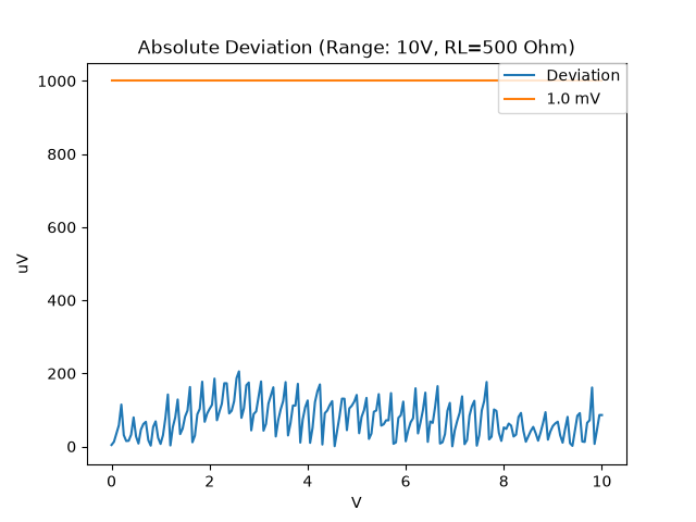
Test Results (RL=500 Ohm)

The diagrams show test runs with a 500 Ohm load connected to the output. The left one is with load correction off, the one on the right is with load correction on.

Load Correction off
Load Correction on

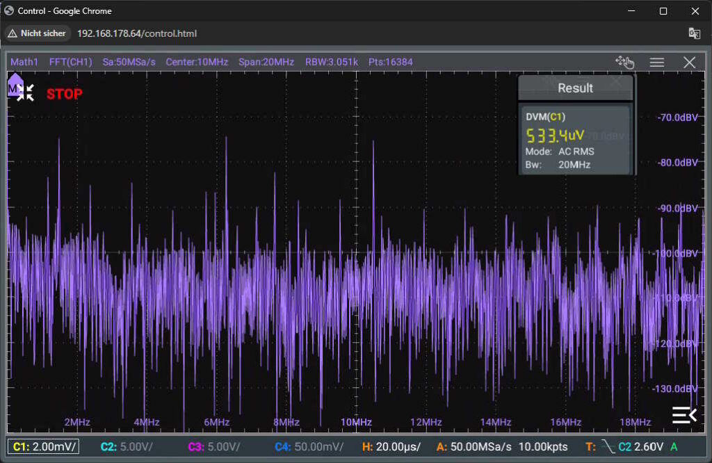
Noise

The noise measured with my DMM (BW=100 kHz) was below 200 uV RMS. My oscilloscope shows around 550 uV RMS if the bandwidth is set to 20 MHz. 

Noise Spectrum @ 10V Output

Offset and Gain

To model an amplifier connected to the output, a user can set its gain and offset parameters. This shifts the plane of reference to the output of the amplifier.

The voltage at the amplifier’s output is modelled as Voltage = EMF * Gain + Offset.

For example, with a gain of 2 the internal EMF is reduced by the same factor but the voltage in the display remains unchanged. By the same logic with an offset of 1V the internal EMF is decreased by 1V.

Limits

To prevent inadvertently outputting a voltage which may damage a connected device the firmware includes a limiting function.

[:SOURce]:LIMits:ENABle[:STATe]?
[:SOURce]:LIMits:LOWer?
[:SOURce]:LIMits:UPPer?

For safety reasons these three parameters are not affected by a *RST or a reset via the GUI. The limits refer to values in the reference plane, i.e. they clip the voltage parameter not the EMF.

MCU, Display and Firmware

For MCU and display I am using the proven combination of a STM32F446RE microcontroller and a 2.8” capacitive touch display.

The firmware uses the framework I have already been using for several other projects. It includes a SCPI parser which interprets commands coming in via one of the composite USB interfaces USBTMC or CDC(serial).

These are the most important commands. For a complete list use command SYSTem:HELP:HEADers?

CommandRemark
[:SOURce]:EMF?/qonly/Get internal EMF.
[:SOURce]:GAIN?Set/get gain factor.
[:SOURce]:LIMits:LOWer?Set/get lower voltage limit.
[:SOURce]:LIMits:UPPer?Set/get upper voltage limit.
[:SOURce]:LIMits:ENABle[:STATe]?Set/get limiting enable state.
[:SOURce]:LOAD:CORRection[:STATe]?Set/get load correction state.
[:SOURce]:LOAD:RESistance?Set/get load resistance. Units: OHM|KOHM| MOHM
[:SOURce]:OFFSet?Set/get offset voltage. Units: V|MV|UV
[:SOURce]:POLarity?UNIPolar|BIPolar
[:SOURce]:RANGe?0.5V|1V|5V|10V|AUTO. In range AUTO the FW uses the narrowest possible range for a given voltage.
[:SOURce]:RANGe:ACTual?/qonly/Get actual range (AUTO)
[:SOURce]:VOLTage?Set/get voltage. Units: V|MV|UV
[:SOURce]:VOLTage:STEP?Step with for UP/DN. Units: V|MV|UV
[:SOURce]:VOLTage:STEP:DN/nquery/Decrease voltage by STEP
[:SOURce]:VOLTage:STEP:UP/nquery/Increase voltage by STEP
ADJustment:GAIN?Set/get gain for current range/polarity combination
ADJustment:OFFSet?Set/get offset for current range/polarity combination. Units: V|MV|UV
ADJustment:RI?Set/get internal resistance in Ohm.
ADJustment:SAVe/nquery/Save calibration data

PCB

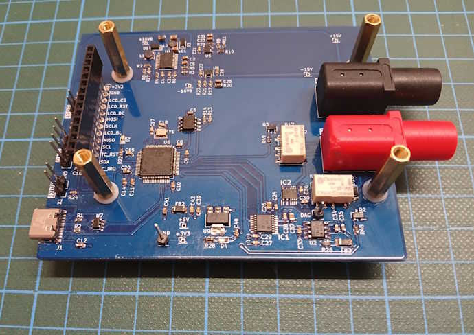
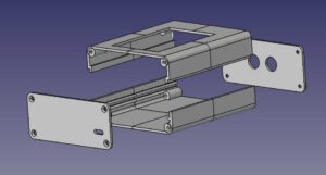
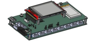
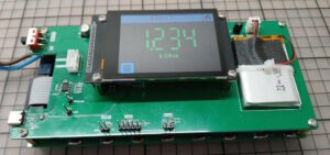
The PCB is a two-layer board with assembly from one side. The display is mounted on top op the main PCB. Power supply and remote control is via the USB-C connector on the left, the voltage output is through two banana jacks on the right. The 100x88x38mm aluminum enclosure is from AliExpress.

Vcal100 PCB

Schematics, Gerber files and firmware can be downloaded from the Download section.