One skill I wanted to learn for a long time was how to program an FPGA. As my recent hardware porjects had turned out really well I now felt ready for this next step.
Every other introduction to FPGA programming starts with the blinking LED example which is not really overwhelming. So to give this a twist I decided to build a multichannel digital pattern generator instead.
Starting out with FPGAs
The first two questions I had to answer before I could try to build anything were:
- Which FPGA family to use (Altera, Xilinx, Lattice, others)?
Should I learn Verilog or VHDL?
The criteria for choosing an FPGA (family) were:
- Chip resources and performance (LUTs, on chip RAM, clock speed)
- Package (no BGA)
- Availability and price
- Easy to integrate with minimal peripheral count
- Tooling, documentation, on line support
After reading a lot of articles, studying datasheets and distributor catalogs I decided to go for Altera’s 10M08 chip. It has 8k logic elements, 384 Kb block memory and requires no external Eeprom for the configuration. It is available in a 144 pin package which I was confident I could solder. The price tag is in the region of 20€ – 30€.
The other question, which language to learn, was easy to answer just by looking at VHDL and Verilog code. Verilog looks very much like C, which I have been using for decades (although I later had to learn that it works quite differently from the sequentially executed C), so I chose Verilog.
First Steps
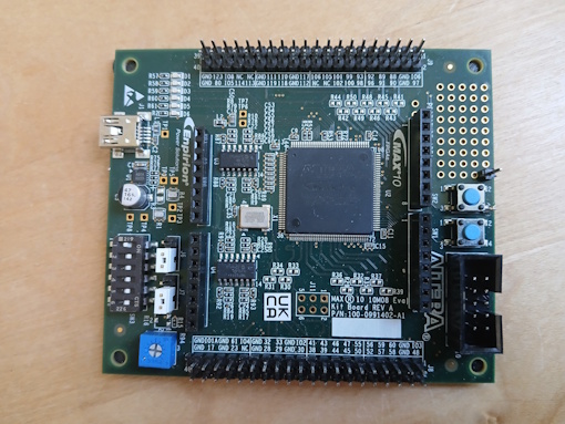
I made my first steps learning Verilog on a 10M08 Eval Kit Board. Unlike some other evaluation boards this board does not have very many peripherals, but gives you easy access to the chip’s GPIO pins which is what I wanted.
Ok, now I had an evaluation board and the Quartus Prime Lite Edition IDE up and running. I was able to write some simple code, burn it into the device and run it. For some serious work however, I wanted to be able to communicate with the FPGA – send commands and receive answers. This was my plan for the next steps to take:
- Write Uart-TX and Uart-RX modules in Verilog
- Use a USB to Uart module to send commands from the PC to the FPGA
- Test by looping back received character
- Write a simple command interpreter on the FPGA
With this simple infrastructure in place I would be able to develop code on the FPGA and, in parallel, write Python code to control the functions on the FPGA. Later on I would translate the Python code to C/C++ so it could be executed on an MCU.
Developing the MCU code on Python first would be faster than having to compile the C code and start up the MCU each time for a single code change.
Download Test Project
For anyone starting on FPGA programming I put the code for the Uart test in an archive which can be downloaded here. The package also contains the Python code to test the FPGA code. The Verilog code contains no Altera specific parts so it should be possible to compile it for FPGAs of any family.
Digital Patterns
A single channel digital pattern is a signal which can take on two values, 0 and 1, represented for example by voltages 0 and 3 V. It can be described by a sequence of value pairs (state1, duration1), (state2, duration2), etc.
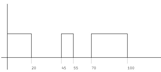
For example, if the time stamps in pattern above are seconds the shown sequence can be represented as (1, 20s), (0, 25s), (1, 10s), (0,15s), (1,30s)
For a representation in a time sampled digital system the time values t must be replaced by the number of samples n = t * fclk where fclk is the clock frequency of the system reading the memory and generating the output.
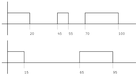
Things get a little bit more complicated when more than one channel must be described.
First, the state variable now has two bits and can take on values from 0..3. Next, when setting up the sequence we must record any state change in any channel and create a new state-value pair. In the example above we get the sequence
(3,15s), (1,5s), (0, 25s), (1,10s), (0,5s), (2,5s), (3,25s), (1,5s)
Quantisation
Because the FPGA reads the memory with a fixed clock, not all time intervals can be represented exactly.
Example:
We want to create a clock signal with frequency 14kHz and the clock frequency is 200 MHz
One period of the signal takes (1/14e3) / (1/200e6) = 200e6/14e3 = 14285.714… clock cycles, which is not integer. Generally, only signals with a period which is an integer multiple of the clock signal’s period can be reproduced exactly. (To be more precise: all time intervals which make up a signal need to be integer multiples of the clock period.) Or put differently, the clock frequency should be an integer multiple of the signal’s frequency. So to be able to create arbitrary signal frequencies we want to be able to change the clock frequency to a matching value.
Periodicity
A channel sequence can be a one time affair or periodic. For a periodic sequence we tell the FPGA to start over from the beginning after reaching the end. For one time signals playback stops after the last sample.
But what happens, if we have more than one channel? These scenarios need to be considered:
- Some channels may be periodic, and others may be one time sequences
- The periods of individual channels may be incongruent.
We may also define the combined sequence to be periodic or not.
As an example let’s assume the combined sequence is to be periodic but some periodic channels have incongruent periods.
Consider the case when period1 = 30 samples and period2 = 50 samples. A periodic overall sequence can be created by repeating sequence1 in memory 5 times and repeating sequence2 in memory 3 times thus making both sequences congruent.
As a second example let’s assume period1=1171 and period2=13831. The least common multiple of 1171 and 13831 is 16196101 equivalent to 13831 periods of channel1 and 1171 periods of channel2. If the FPGA’s memory is large enough for the required transitions (2 for every channel period) the signal can be created, otherwise the periods are incongruent and the combined signal cannot be produced.
Tweaking the Clock Frequency
One way to overcome the limitations described above is to find a sampling frequency which allows the incongruent periods to become congruent.
Example:
Fclk = 200MHz
F1 = 5 kHz
n1 = 200MHz/5kHz = 40000
Fclk = 210MHz
F2 = 7 kHz
n2 = 210MHz/7kHz = 30000
Individually, both signals can be created exactly. However, for this they require different clock frequencies. To create both signals simultaneously we need to find a clock frequency which fits both.
Let’s try
Fclk = 256.41MHz
n1 = 256.41MHz/5kHz = 51282
n2 = 256.41MHz/7kHz = 36630
Obviously, if we can find a clock frequency Fclk for which both Fclk/F1 and Fclk/F2 are integers then F1 and F2 can be produced without errors.
Depending on the properties of its PLL the FPGA can generate only a limited set of discrete clock frequencies. So this approach can solve some but not all conflicts between incongruent signal periods.
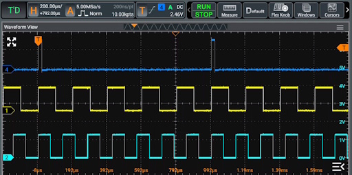
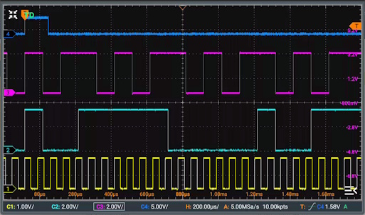
The screenshot above shows how these two signals would be represented in the FPGA’s memory. The dark blue trace at the top is the Marker output which signals the beginning of a period. 5 periods of the 5 kHz signal1 and 7 periods of the 7kHz signal2 fit into the 1ms period which is stored in memory. This requires 22 transition entries in memory.